 By Jackson Mike
Introduction
A successful electronic product begins long before manufacturing starts. While advanced equipment, skilled technicians, and quality inspection systems play critical roles in production, the foundation of every reliable PCB assembly is an optimized circuit board design.
Even the most experienced turnkey PCB assembly provider can face challenges if the PCB design contains layout errors, poor component placement, inadequate routing, or manufacturability issues. A design that looks functional on a computer screen may still create assembly difficulties, production delays, and reliability problems during manufacturing.
As electronic devices become increasingly compact and sophisticated, PCB design quality has a greater impact on manufacturing success than ever before. Well-designed PCBs improve production efficiency, reduce costs, enhance product reliability, and accelerate time-to-market.
Understanding how PCB design influences turnkey PCB assembly helps engineers, product developers, and manufacturers create products that perform reliably while supporting efficient manufacturing processes.
What Is Turnkey PCB Assembly?
Turnkey PCB assembly is a complete manufacturing solution where one provider manages all stages of PCB production.
Typical services include:
- PCB fabrication
- Component sourcing
- SMT assembly
- Through-hole assembly
- Inspection and testing
- Final packaging and delivery
Because a turnkey manufacturer oversees the entire production process, PCB design quality directly affects every stage of manufacturing.
A well-optimized design helps manufacturers achieve higher yields, fewer defects, and smoother production workflows.
Why PCB Design Matters in Manufacturing
PCB design serves as the blueprint for fabrication and assembly.
Every manufacturing process depends on the information contained within the PCB layout, including:
- Component placement
- Copper routing
- Drill locations
- Layer stack-up
- Solder mask specifications
- Mechanical dimensions
Errors at the design stage often become more expensive and difficult to correct once production begins.
Consequences of Poor PCB Design
Design flaws can result in:
- Assembly defects
- Signal interference
- Thermal problems
- Manufacturing delays
- Product failures
- Increased production costs
Optimizing the design before fabrication significantly improves production outcomes.
Design for Manufacturing (DFM): The First Step Toward Success
One of the most important aspects of PCB design is Design for Manufacturing (DFM).
DFM focuses on creating PCB layouts that can be manufactured efficiently and consistently.
Key DFM Considerations
Manufacturers evaluate:
- Trace widths and spacing
- Drill sizes
- Via placement
- Copper balancing
- Panelization requirements
- Solder mask clearances
Benefits of DFM
Proper DFM implementation helps:
- Reduce fabrication defects
- Improve assembly yields
- Lower production costs
- Minimize rework
- Increase manufacturing speed
Many turnkey PCB assembly providers perform DFM reviews before production begins to identify potential issues early.
Component Placement and Assembly Efficiency
Component placement has a direct impact on assembly quality and manufacturing efficiency.
Poor placement can create numerous problems during SMT and through-hole assembly.
Common Placement Issues
Examples include:
- Components positioned too closely together
- Inconsistent orientation
- Insufficient clearance for soldering
- Difficult inspection access
These issues can reduce assembly accuracy and increase defect rates.
Best Practices for Component Placement
Effective layouts typically feature:
- Consistent component orientation
- Adequate spacing
- Logical grouping of related circuits
- Easy access for testing and inspection
Optimized placement improves assembly speed and product reliability.
Surface Mount Technology (SMT) Compatibility
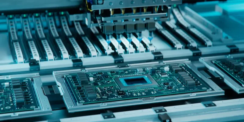
Modern turnkey PCB assembly relies heavily on Surface Mount Technology (SMT).
SMT enables automated placement of miniature components at high speed and precision.
Design Factors Affecting SMT Assembly
Manufacturers evaluate:
- Pad dimensions
- Component spacing
- Fiducial placement
- Solder paste accessibility
Improper SMT design can lead to defects such as:
- Tombstoning
- Solder bridges
- Misaligned components
- Incomplete solder joints
Designs optimized for SMT improve manufacturing consistency and quality.
Trace Routing and Signal Integrity
PCB routing affects both electrical performance and manufacturability.
Poor routing decisions can introduce signal quality problems that impact product functionality.
Common Routing Problems
Issues may include:
- Excessive trace length
- Crosstalk
- Impedance mismatches
- Inadequate grounding
- Signal reflections
Improving Signal Integrity
Effective routing strategies include:
- Controlled impedance traces
- Proper ground planes
- Short signal paths
- Differential pair routing where required
Strong signal integrity improves overall product performance and reliability.
Thermal Management Considerations
Heat is one of the most common causes of electronic component failure.
Poor thermal design can reduce product lifespan and create operational instability.
Sources of Thermal Problems
Examples include:
- High-power components
- Dense layouts
- Insufficient copper area
- Poor airflow planning
Design Strategies for Heat Dissipation
Manufacturers often recommend:
- Thermal vias
- Copper pours
- Heat sinks
- Strategic component placement
Proper thermal management supports long-term reliability and manufacturing success.
Layer Stack-Up Design
Modern electronic products frequently use multi-layer PCBs to support complex circuitry and compact designs.
Importance of Layer Stack-Up
The layer structure influences:
- Signal integrity
- Electromagnetic compatibility
- Thermal performance
- Manufacturing complexity
Stack-Up Optimization
Well-designed stack-ups help:
- Reduce noise
- Improve routing efficiency
- Enhance reliability
- Simplify fabrication
Collaborating with a turnkey PCB assembly provider during stack-up planning can improve manufacturability.
Via Design and Manufacturing Reliability
Vias connect electrical signals between PCB layers.
While essential, poor via design can create manufacturing and performance problems.
Common Via Issues
These include:
- Incorrect drill sizes
- Excessive via density
- Weak annular rings
- Poor placement
Best Practices
Proper via design improves:
- Electrical connectivity
- Thermal management
- Structural reliability
- Fabrication yields
Manufacturers often provide recommendations to optimize via structures during DFM reviews.
Solder Mask and Silkscreen Design
Solder mask and silkscreen layers contribute significantly to assembly quality.
Solder Mask Functions
The solder mask:
- Prevents solder bridging
- Protects copper traces
- Improves insulation
Common Solder Mask Errors
Problems include:
- Inadequate clearance
- Misalignment
- Excessive mask openings
Silkscreen Importance
Silkscreen markings help with:
- Component identification
- Assembly guidance
- Inspection procedures
- Maintenance activities
Clear labeling improves manufacturing efficiency and troubleshooting.
Testability and Inspection Accessibility
A PCB must be designed not only for functionality but also for testing.
Testing accessibility becomes especially important during large-scale production.
Design for Testability (DFT)
DFT principles include:
- Accessible test points
- Probe clearance
- Functional testing support
- Inspection visibility
Benefits of DFT
Improved testability helps:
- Detect defects earlier
- Reduce troubleshooting time
- Improve quality assurance
- Increase production yields
Designs optimized for testing support more efficient manufacturing operations.
Impact on Production Costs
Design quality directly influences manufacturing expenses.
Poorly designed PCBs often require:
- Additional engineering reviews
- Manual assembly adjustments
- Rework procedures
- Extra testing
These activities increase production costs and delay project completion.
Cost Benefits of Good Design
Optimized PCB layouts help reduce:
- Scrap rates
- Assembly errors
- Material waste
- Production delays
Efficient designs improve both profitability and manufacturing efficiency.
Faster Time-to-Market Through Better Design
Time-to-market is a major competitive factor in modern electronics industries.
Design-related manufacturing issues can delay product launches significantly.
How Good Design Accelerates Production
Well-prepared PCB layouts support:
- Faster DFM approval
- Efficient fabrication
- Smooth assembly operations
- Reduced engineering revisions
This helps businesses introduce products to market more quickly.
The Importance of Collaboration With Manufacturers
Successful PCB development often involves close collaboration between designers and manufacturers.
Experienced turnkey PCB assembly providers can offer valuable guidance during the design phase.
Areas of Manufacturer Support
Manufacturers may assist with:
- DFM recommendations
- DFA analysis
- Material selection
- Thermal optimization
- Component sourcing guidance
Early collaboration reduces manufacturing risks and improves product quality.
Industries Where Design Quality Is Critical
PCB design quality affects every electronics sector, including:
Medical Devices
Require high reliability and regulatory compliance.
Automotive Electronics
Demand durability and long-term performance.
Telecommunications
Need excellent signal integrity and high-speed operation.
Aerospace Systems
Require precision manufacturing and extreme reliability.
Consumer Electronics
Focus on miniaturization, cost efficiency, and mass production.
In each industry, design quality directly influences manufacturing success.
Future Trends in PCB Design Optimization
PCB design tools continue to evolve alongside manufacturing technology.
Emerging innovations include:
- AI-assisted PCB design
- Automated DFM analysis
- Real-time manufacturability simulation
- Digital twin technology
- Advanced thermal modeling
These technologies help engineers identify potential manufacturing issues before production begins.
Choosing a Turnkey PCB Assembly Partner That Supports Design Optimization
Not all manufacturers provide the same level of engineering support.
Businesses should look for providers that offer:
- Comprehensive DFM reviews
- DFA optimization services
- Engineering consultation
- Advanced testing capabilities
- Modern manufacturing equipment
Strong design support can significantly improve production outcomes.
Conclusion
PCB design quality is one of the most important factors influencing turnkey PCB assembly success. A well-designed PCB improves manufacturability, reduces defects, lowers production costs, enhances reliability, and accelerates time-to-market.
From component placement and signal routing to thermal management and testing accessibility, every aspect of PCB design affects manufacturing performance.
By following DFM and DFA principles and collaborating closely with experienced turnkey PCB assembly providers, businesses can create products that are easier to manufacture, more reliable in operation, and better prepared for long-term production success.
As electronics continue to become more advanced and compact, high-quality PCB design will remain a critical competitive advantage in modern manufacturing.